
AR Waveguide Manufacturing for AI Glasses
Augmented Reality (AR) waveguides are the optical heart of AI glasses. These thin, transparent components carry the image from a miniature light engine to the wearer’s eye. Learn how AR waveguides work, how they are manufactured, and how large-area nanoimprint lithography enables cost-effective volume production.
What is an AR waveguide and how does it work?
An AR Waveguide is a flat, optical component usually made of high-refractive-index glass or, in some designs, polymer.
It guides light by total internal reflection (TIR). In a diffractive waveguide, a light engine (based on LCoS, DLP, microLED or laser beam scanning) sends a collimated image into the waveguide through a nanostructured in-coupling grating. The light then travels through the substrate by TIR. Further gratings expand it across a larger area and gradually couple it out toward the eye, so the wearer sees digital content overlaid on the real world.
An ideal AR display combines a wide field of view (FOV), a large eyebox, high brightness, and good uniformity and color balance. Many of these properties depend strongly on how accurately the grating nanostructures are replicated.
Waveguides and their optical architectures
AR waveguides use several optical architectures, each with different design and manufacturing requirements. Morphotonics’ Roll-to-Plate nanoimprint lithography platform is designed to manufacture surface-relief grating (SRG) waveguides at scale. The overview below places SRG technology within the broader AR waveguide landscape.
Diffractive waveguides (SRG)
Surface relief gratings (binary, slanted, blazed or multi-level) diffract light into and out of the waveguide. Slanted and blazed profiles raise efficiency but are the hardest to replicate faithfully. SRG is one of the most widely adopted waveguide architectures in AR glasses and is well suited to nanoimprint replication.
Holographic and polarization waveguide
Refractive index modulation inside a film (HOE) or liquid-crystal-based polarisation gratings offer high efficiency in narrow spectral bands, with tighter process-window and environmental constraints.
Metasurface and hybrid designs
Sub-wavelength pillar arrays and 2D crossed gratings compress the optical stack and can combine pupil expansion functions in a single layer.
Reflective and geometric waveguides
Arrays of embedded semi-reflective mirrors give excellent colour fidelity but rely on precision bonding and dicing rather than nanopatterning, which limits cost scaling.
Morphotonics bridges the gap between qualified optical designs and repeatable production through large-area Roll-to-Plate nanoimprint lithography, multi-wafer processing and automated manufacturing platforms.
From high-performing optics to manufacturable AR waveguides
AR waveguide performance begins with optical design, but commercial success depends on manufacturing. Surface relief gratings must be replicated with tight control over geometry, residual layer thickness, pitch, overlay and defects across every substrate.
As volumes grow, small variations can affect image uniformity, efficiency and yield. The challenge is not making one high-quality waveguide, but producing many identical ones at the throughput and cost that mainstream AR glasses and display-equipped AI glasses require.
Morphotonics addresses this scale-up challenge for SRG waveguides with Roll-to-Plate nanoimprint lithography on panel-sized carriers that combines precise replication, multi-wafer handling and an industrial production architecture.
Four priorities for volume waveguide production
Replication fidelity
Transfer validated nanoscale grating structures accurately and repeatably.
Yield and defect control
Maintain process consistency across many waveguides and across the full carrier area.
Throughput and cost
Increase the number of good waveguides per cycle while reducing handling steps and process overhead.
Process flexibility
Support different grating geometries, substrate formats, resins and downstream process routes.
Morphotonics’ Nanoimprint lithography for scalable AR waveguide production
Nanoimprint lithography reproduces micro- and nanostructures from a master using a patterned stamp and a UV-curable resin. Instead of directly patterning every waveguide with the original master-fabrication process, a qualified structure can be replicated repeatedly onto production substrates.
Morphotonics’ proprietary Roll-to-Plate (R2P) nanoimprint technology uses a flexible stamp and controlled rolling contact to replicate structures across small and large substrate formats. For AR waveguide manufacturing, the process is applied to multi-wafer carriers so several round or square substrates can be handled within one production architecture.
The imprinted layer can function as a permanent optical structure or as a precise etch mask for downstream processing, depending on the waveguide design and integration route.
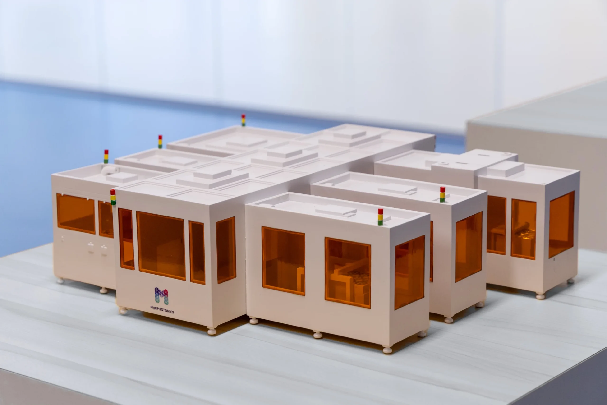
Cypris X700
A platform for AI Glasses
Cypris X700 is a fully automated, modular nanoimprint production platform developed for scalable waveguide manufacturing. It integrates Roll-to-Plate nanoimprint lithography with high-resolution inkjet deposition, robotic handling and multi-wafer carriers to improve throughput, precision and production consistency.
The platform accommodates round wafers and square glass formats, with carrier handling sizes up to 700 x 700 mm. By processing several substrates within one carrier architecture, Cypris is designed to support cost-efficient production as AR and AI glasses move toward mainstream volumes.
| Specification | Value |
|---|---|
| Substrate size | Up to 700 mm × 700 mm |
| Carrier formats | 4 × 300 mm or 9 × 200 mm round wafers; square glass capable |
| Substrate thickness | 0.3–1.1 mm |
| TAKT time | 4 minutes possible; product-texture dependent |
| Handling | Automated multi-wafer carriers and robotic substrate handling |
| Annual capacity | Up to 6 million eyepieces |
Why Roll-to-Plate for AR waveguides?
01
Panel-based substrate utilization supports multiple wafers or square glass formats in one carrier.
02
Flexible stamp technology supports replication of complex surface relief grating geometries.
03
Controlled rolling contact enables high-fidelity imprinting across a large processing area.
04
Modular process integration supports permanent optical layers and etch-mask routes.
05
Automation reduces manual handling as production moves toward higher volumes.
Frequently asked questions
-
Nanoimprint lithography (NIL) is a high-resolution nanofabrication technique used to create micro- and nano-scale surface patterns by physically replicating structures from a stamp (mold) into a functional material. It is widely used for applications that require precise and uniform patterning over large areas, such as optical components and functional surfaces.
Ready to scale nanostructures?
Connect with Morphotonics’ nanoimprint specialists to explore how large-area Roll-to-Plate nanoimprint lithography can bring your optical or functional design into volume production.